

- Home
- /
- Products
- /
- Texas Instruments
- /
- General
- /
- General
- /
- CD4066-BE – Texas Instruments
CD4066-BE – Texas Instruments
Buy CD4066-BE – Texas Instruments online, Order today to get instant delivery in all over india.
Out of Stock
You're on the list! We'll email you when this product is back in stock.
Enter your email to be notified when this product is available again.
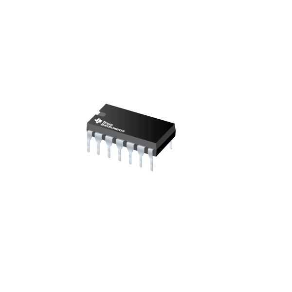
The CD4066B device is a quad bilateral switch intended for the transmission or multiplexing of analog or digital signals. It is pin-for-pin compatible with the CD4016B device but exhibits a much lower on-state resistance. In addition, the on-state resistance is relatively constant over the full signal-input range.
The CD4066B device consists of four bilateral switches, each with independent controls. Both the p and the n devices in a given switch are biased on or off simultaneously by the control signal. As shown in Figure 17, the well of the n-channel device on each switch is tied to either the input (when the switch is on) or to VSS (when the switch is off). This configuration eliminates the variation of the switch-transistor threshold voltage with the input signal and, thus, keeps the on-state resistance low over the full operating-signal range.
The advantages over single-channel switches include peak input-signal voltage swings equal to the full supply voltage and more constant on-state impedance over the input-signal range. However, for sample-and-hold applications, the CD4016B device is recommended.
Features and Specifications:
- 15-V Digital or ±7.5-V Peak-to-Peak Switching
- 125-Ω Typical On-State Resistance for 15-V Operation
- Switch On-State Resistance Matched to Within 5 Ω Over 15-V Signal-Input Range
- On-State Resistance Flat Over Full Peak-to-Peak Signal Range
- High On or Off Output-Voltage Ratio: 80 dB Typical at fis = 10 kHz, RL = 1 kΩ
- High Degree of Linearity: <0.5% Distortion Typical at fis = 1 kHz, Vis = 5-Vp-p VDD – VSS ≥ 10-V, RL = 10 kΩ
- Extremely Low Off-State Switch Leakage, Resulting in Very Low Offset Current and High Effective Off-State Resistance: 10 pA Typical at VDD – VSS = 10-V, TA = 25°C
- Extremely High Control Input Impedance (Control Circuit Isolated From Signal Circuit): 1012 Ω Typical
- Low Crosstalk Between Switches: –50 dB Typical at fis = 8 MHz, RL = 1 kΩ
- Matched Control-Input to Signal-Output Capacitance: Reduces Output Signal Transients
- Frequency Response, Switch On = 40 MHz Typical
- 100% Tested for Quiescent Current at 20-V
- 5-V, 10-V, and 15-V Parametric Ratings
Package Includes:
1 x CD4066-BE 20-V 1:1 (SPST) 4-channel analog switch IC
welcome
welcome
You May Also Like
View all →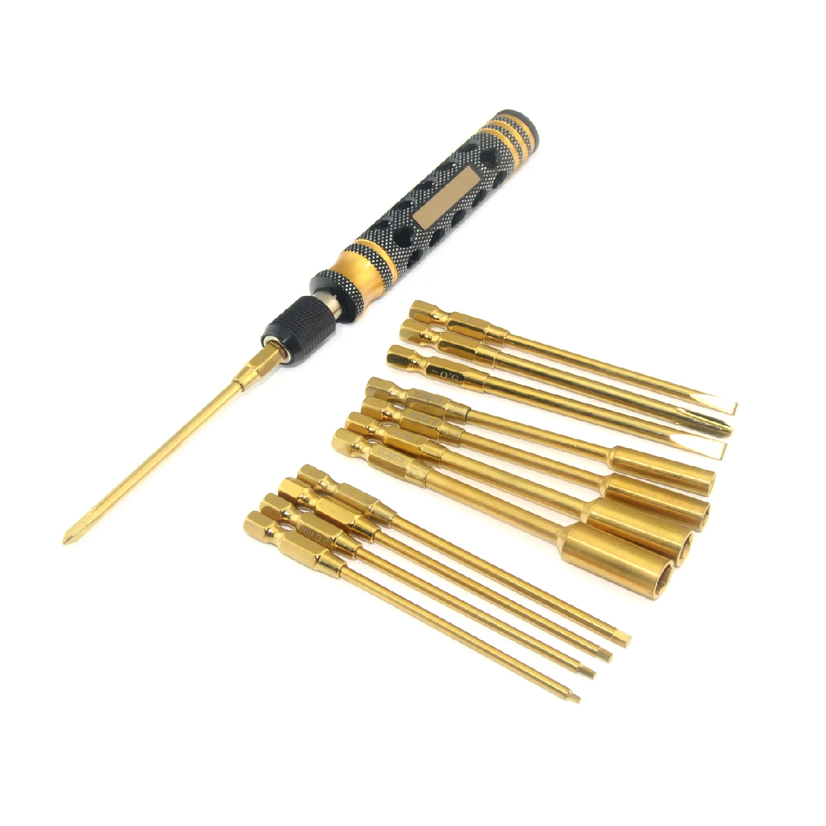
12IN1 RC Tools Kit
₹ 3,103.85
Buy 12IN1 RC Tools Kit online, Order today to get instant delivery in all over india.

HOKI M3 Digital Multimeter
₹ 1,383.45
Buy HOKI M3 Digital Multimeter online, Order today to get instant delivery in all over india.
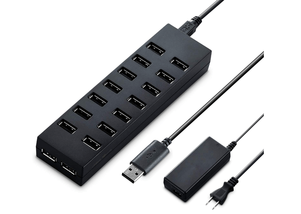
Elecom U2H-Z16SBK 16 Port USB Hub
₹ 1,564.00
Buy Elecom U2H-Z16SBK 16 Port USB Hub online, Order today to get instant delivery in all over india.

Buy Waveshare IMX219-200 Camera, 200° FOV, Applicable for Jetson Nano online, Order today to get instant delivery in all over india.