-
 Fast Shipping
Get the Priority Shipping on Prepaid Orders
Prepaid Orders
-
 Normal Shipping
 Get Normal Delivery (Surface) with Cash On Delivery
COD Orders


₹17.65 Original price was: ₹17.65.₹16.28Current price is: ₹16.28. (Including tax)
Discount per Bulk Quantity
| Quantity | Discount | Price |
|---|---|---|
| 5 - 10 | 5% | ₹15.47 (Including tax) |
| 11 - 20 | 8% | ₹14.98 (Including tax) |
| 21 - 40 | 10% | ₹14.66 (Including tax) |
| 41 - 100 | 12% | ₹14.32 (Including tax) |
Out of stock
No worries! Enter your email, and we'll let you know as soon as it's back in stock.
Get the Priority Shipping on Prepaid Orders
Prepaid Orders
Get Normal Delivery (Surface) with Cash On Delivery
COD Orders
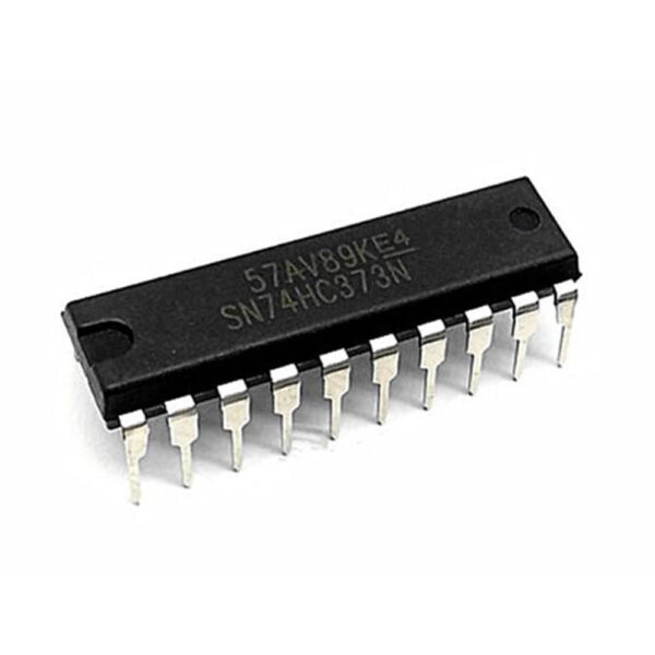
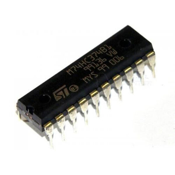
74HC series ICs are High-speed logic gates with very low power consumption that utilize advanced silicon-gate CMOS technology and 74HC374 is one of them. 74HC374 ICs contain eight positive-edge-triggered D-type flip-flops with 3-Output states i.e. High, Low, and High Impedance. Which is designed specifically for driving highly capacitive or relatively low-impedance loads. High Impedance comes to active low enable pin of these ICs where output-enable (OE)’ input places the eight outputs in either a normal logic state (high or low logic levels) or the high-impedance state. (OE)’ does not affect the internal operations of the flip-flops. Old data can be retained or new data can be entered while the outputs are in the high-impedance state.

The 74HC374 ICs have a wide operating range of VCC from 2 V to 6 V. Maximum current consumption is 80 uA through Icc and 1 uA per input pin. And the propagation delay is 14 ns. They can drive 10 LS-TTL loads at a time. Which means that the output pin of D-type flip-flop can drive 10 TTL based Low-Power Schottky( LS ) input pins. They can provide 6 mA on outputs at 5 V VCC. They allow inputs and outputs up to VCC. Recommended operating VCC is 5 V. Load Current can reach up to 35 mA per output pin and 70 mA for overall pins in between 0 V to VCC.
Specification:
| Operating Voltage Range | 2.0 to 6.0 V |
| Package | DIP−20 |
| Input Current | 1 uA |
| Powering Current | 80 uA |
| Output Current at VCC | 6 mA |
| Fan-Out | 10 LS-TTL Load |
| Propagation Delay | 14 ns |
| Temperature Range | -65 °C to +150 °C |
Pin Configuration:
| Data Input (D[0:7]) | 3, 4, 7, 8, 13, 14, 17, 18 |
| Output Pins (Q[0:7]) | 2, 5, 6, 9, 12, 15, 16, 19 |
| Active Low Enable (OE’) | 1 |
| Clock (CLK) | 11 |
| Power Supply (VCC) | 20 |
| Ground (GND) | 10 |
| Country of Origin | China |
| Weight | 1 kg |
|---|
Only logged in customers who have purchased this product may leave a review.
Shipping and Delivery Policy
1. Shipping Process:
2. Shipping Charges:
3. Order Tracking:
4. Delivery Address:
5. Delivery Issues:
6. No Return Policy for Opened/Soldered Products:
7. Refund Policy:
Out of stock
Out of stock
Out of stock
Out of stock
Out of stock
Out of stock
Out of stock
Out of stock
No account yet?
Create an Account
Out of stock
Reviews
Clear filtersThere are no reviews yet.